API
analysis
fem
Functions for doing FEM analysis of gdsfactory/qnngds geometries
- class qnngds.analysis.fem.Result(mesh, element, sigma, A, u)[source]
Bases:
objectClass for storing results of FEM simulation
- __init__(mesh, element, sigma, A, u)[source]
Constructor for Result
- Parameters:
mesh (MeshTri1) – skfem mesh (first-order triangular mesh)
element (ElementTriP3) – piecewise cubic element
sigma (np.ndarray) – conductivity for each dof
A (scipy.sparse.csr_matrix) – discretized linear system
u (dict[tuple[str,str], np.ndarray]) – solution vector for each port pair
- qnngds.analysis.fem.get_squares(result: Result) dict[str, float][source]
Calculate number of squares from result generated by solve_laplace
- qnngds.analysis.fem.visualize_current(result: Result, port_pair: tuple[str, str], normalize: bool = True, ax=None)[source]
Visualize current density of result generated by solve_laplace
- Parameters:
result (Result) – result obtained from running solve_laplace on a mesh
port_pair (tuple[str, str]) – pair of ports to visualize
normalize (bool) – default True, if False plot the un-normalized current in A/um
ax (plt.axis | None) – existing plot axis to add plot to if not None.
- Returns:
(plt.axis)
- qnngds.analysis.fem.visualize_mesh(mesh, ax=None)[source]
Visualize mesh of wire/component
- Parameters:
mesh (MeshTri1) – scikit fem mesh
ax (plt.axis | None) – existing plot axis to add plot to if not None.
- Returns:
(plt.axis)
- qnngds.analysis.fem.visualize_boundaries(mesh, ax=None)[source]
Visualize boundaries of wire/component
- Parameters:
mesh (MeshTri1) – scikit fem mesh
ax (plt.axis | None) – existing plot axis to add plot to if not None.
- Returns:
(plt.axis)
- qnngds.analysis.fem.make_mesh(device: Device, layer: str | int | tuple[int, int], tolerance: float = 0.01)[source]
Generate a mesh from a qnngds.Device
- Parameters:
device (qnngds.Device) – input device to make a mesh of
layer (LayerSpec) – layer of device to use.
tolerance (float) – simplify tolerance for geometry to reduce mesh complexity
- Returns:
(MeshTri1) mesh of the device
superscreen
Functions for interfacing with superscreen
- qnngds.analysis.superscreen.make_superscreen_device(device: Device, london_lambda: dict[str | int | tuple[int, int], float] | float, thickness: dict[str | int | tuple[int, int], float] | float, z0: dict[str | int | tuple[int, int], float] | None = None, min_refine_points: int = 100) Device[source]
Make a superscreen.Device that can be used for simulation from a qnngds Device.
Makes a best-effort attempt to autoassign ports to different polygons in the geometry. Cannot currently model structures with holes in them.
- Parameters:
device (qnngds.Device) – input device. Supports multiple layers and ports, although self-intersecting layers with ports may not be processed correctly.
london_lambda (dict[LayerSpec, float] | float) – per-layer london magnetic penetration depth in microns (if dict), or same penetration depth for all layers (if float)
thickness (dict[LayerSpec, float] | float) – per-layer thickness of the film in microns (if dict), or same thickness for all layers
z0 (dict[LayerSpec, float] | None) – optional, z height of each layer. Required for multiple layer device. Default None.
min_refine_points (int) – default 100, minimum number of points for polygon.refine()
- Returns:
(superscreen.Device) –
- a superscreen.Device instance that can be used with the superscreen modeling
kit to simulate flux trapping, fluxoids, mutual inductance, and other screening effects.
tdgl
Functions for interfacing with py-tdgl
- qnngds.analysis.tdgl.make_tdgl_device(device: Device, coherence_length: float, london_lambda: float, thickness: float, gamma: float, layer: str | int | tuple[int, int]) Device[source]
Make a tdgl.Device that can be used for simulation from a qnngds Device.
Cannot currently model structures with holes in them.
- Parameters:
device (qnngds.Device) – input device. Only one layer will be used, supports multiple ports, but regions must be contiguous(?)
layer (LayerSpec) – layer of device to use.
coherence_length (float) – coherence length of superconducting film in microns
london_lambda (float) – london magnetic penetration depth in microns
thickness (float) – thickness of the film in microns
gamma (float) – material constant describing ratio of scattering time for electrons and phonons
- Returns:
(tdgl.Device) –
- a tdgl.Device instance that can be used with tdgl.solve() to model evolution of
order parameter and phase under application of bias current.
decorator
Define a registry for devices. Currently this is only used for documentation purposes.
- qnngds.decorator.device(f)[source]
Decorator to register DeviceFactories into the global variable qnngds.decorator._devices.
This is currently used for documentation purposes, however it would be nice to replicate some of the functionality of kfactory to overwrite the device name based on the arguments supplied to the function.
For example, if we wish to define a new DeviceFactory that can be used to generate Devices, we can write the following:
 1import qnngds as qg
 2from qnngds import Device
 3
 4@qg.device
 5def my_new_device(
 6    some_param: int,
 7    some_other_param: str,
 8    layer: LayerSpec,
 9    ...
10) -> Device:
11    """Docstring to explain my function.
12
13    Parameters
14        some_param (int): explanation of some_param.
15        some_other_param (str): explanation of some_other_param.
16        layer (LayerSpec): GDS layer specification.
17        ...
18
19    Returns
20        (Device): description of the device returned
21    """
22    ...
devices
Devices module contains variations of common devices used in the circuits designed by QNN group.
diode
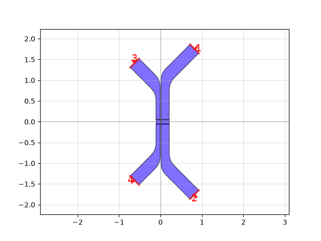
Layout for superconducting diode [1].
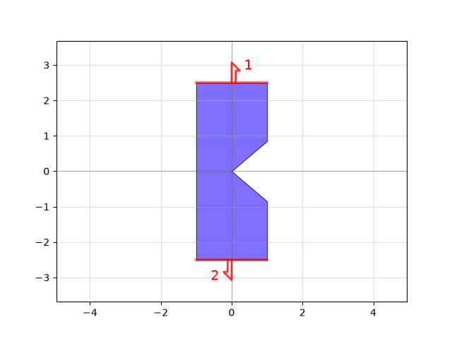
- qnngds.devices.diode.basic(width: float = 2, notch_depth: float = 1, notch_angle: float = 90, length: float = 5, mirror: bool = False, layer: LayerSpec = (1, 0)) Device[source]
Create notched vortex diode on single layer
- Parameters:
width (float) – wire width in microns
notch_depth (float) – amount notch protrudes into wire
notch_angle (float) – angle of notch opening in degrees
length (float) – length of device
mirror (bool) – if True, place notch on left side
layer (LayerSpec) – GDS layer specification
- Returns:
(Device) – the diode
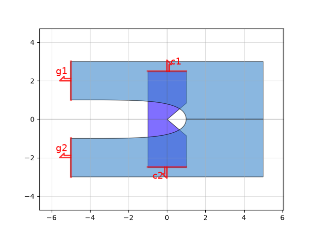
- qnngds.devices.diode.gated(channel_spec: DeviceSpec = <function basic>, gate_spec: DeviceSpec = functools.partial(<function optimal_hairpin>, width=2, pitch=4, turn_ratio=2, layer=(10, 0))) Device[source]
Create notched vortex diode with a gate.
Lateral offset of the gate can be done by first offsetting the gate before passing it as an argument to this function.
- Parameters:
channel_spec (DeviceSpec) – what to use for diode channel (e.g. diode.basic)
gate_spec (DeviceSpec) – what to use for top gate (e.g. geometries.optimal_hairpin)
- Returns:
(Device) – the gated diode
htron
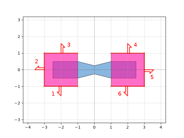
Heater cryotron devices [1], [2].
- qnngds.devices.htron.heater(heater_spec: DeviceSpec = Device (name "nw_sharp" (uid 2), ports [1, 2], aliases [], 0 polygons, 1 references), pad_size: tuple[float, float] = (2, 2), pad_layer: LayerSpec = (20, 0)) Device[source]
Create a heater with superconducting leads for use with hTrons.
- Parameters:
heater_spec (DeviceSpec) – spec for heater
pad_size (tuple[float, float]) – (width, height) of pad
pad_layer (LayerSpec) – layer specification for top pads
- Returns:
(Device) – a heater with pads
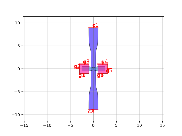
- qnngds.devices.htron.multilayer(rotation: float = 0, channel_spec: DeviceSpec = functools.partial(<function variable_length>, constr_width=1, wire_width=2, length=4, symmetric=True, layer=(1, 0)), gate_spec: DeviceSpec = <function heater>) Device[source]
Create a multilayer hTron.
- Parameters:
rotation (float) – amount to rotate gate relative to channel.
channel_spec (DeviceSpec) – callable function that generates a Device for the channel nanowire
gate_spec (DeviceSpec) – callable function that generates a Device for the gate nanowire
- Returns:
(Device) – a multilayer hTron
- qnngds.devices.htron.planar(wire_width: int | float = 0.3, gate_width: int | float = 0.1, channel_width: int | float = 0.2, gap: int | float = 0.02, gate_length: int | float = 0.01, channel_length: int | float = 0.01, layer: LayerSpec = (1, 0)) Device[source]
Create a planar hTron.
- Parameters:
wire_width (int or float) – Width of routing wires in microns
gate_width (int or float) – Width of superconducting gate in microns
channel_width (int or float) – Width of superconducting channel in microns
gap (int or float) – Spacing between gate and channel in microns
gate_length (int or float) – Length of superconducting gate in microns
channel_length (int or float) – Length of superconducting channel in microns
layer (LayerSpec) – GDS layer specification
- Returns:
(Device) – a single planar hTron
nanowire
Single nanowire constriction.
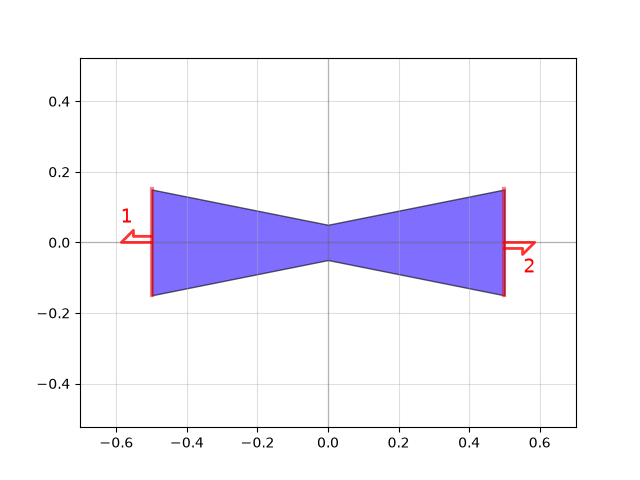
- qnngds.devices.nanowire.sharp(constr_width: float = 0.1, wire_width: float = 0.3, length: float = 1, layer: LayerSpec = (1, 0)) Device[source]
Creates a single wire, made of two linear tapers starting at wire_width tapering down to constriction of width constr_width.
- Parameters:
constr_width (int or float) – The width of the channel (at the hot-spot location).
wire_width (int or float) – The width of connections to source/drain
length (int or float) – The length of the interior constriction.
layer (LayerSpec) – GDS layer specification
- Returns:
(Device) – sharp constriction
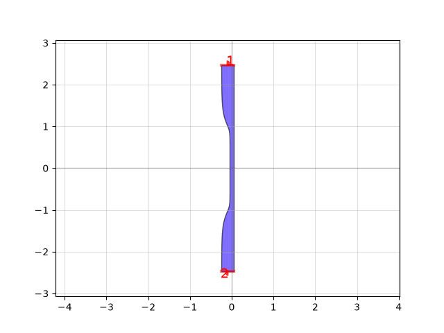
- qnngds.devices.nanowire.variable_length(constr_width: float = 0.1, wire_width: float = 0.3, length: float = 1, num_pts: int = 100, symmetric: bool = False, layer: LayerSpec = (1, 0)) Device[source]
Creates a single wire, made of two optimal steps from constr_width to wire_width with a constriction of the chosen length in the middle.
- Parameters:
constr_width (int or float) – The width of the channel (at the hot-spot location).
wire_width (int or float) – The width of connections to source/drain
length (int or float) – The length of the interior constriction.
num_pts (int) – The number of points comprising the optimal_steps geometries.
symmetric (bool) – if True, symmetric taper between constr_width and wire_width
layer (LayerSpec) – GDS layer specification
- Returns:
(Device) – 2 optimal steps to/from a narrow wire.
- Raises:
ValueError if constr_width > wire_width –
ntron
Nanocryotron [1] variants.
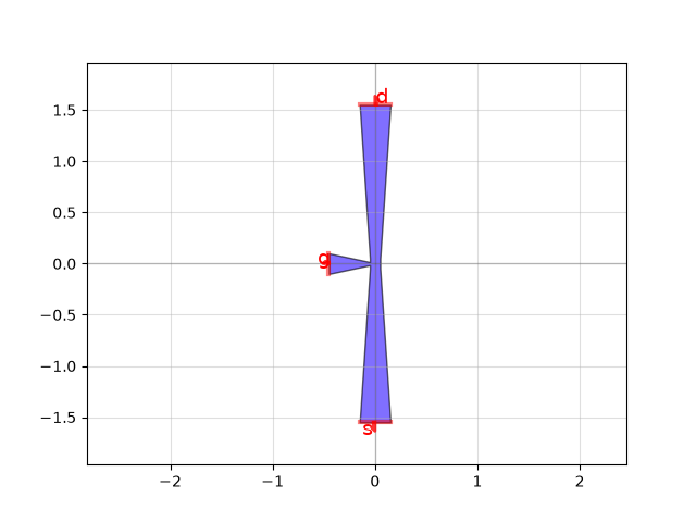
- qnngds.devices.ntron.sharp(choke_w: float = 0.03, gate_w: float = 0.2, channel_w: float = 0.1, source_w: float = 0.3, drain_w: float = 0.3, gate_sq: float = 2, channel_sq: float = 1, source_sq: float = 5, drain_sq: float = 5, symmetric: bool = True, layer: LayerSpec = (1, 0)) Device[source]
Creates a sharp ntron device.
- Parameters:
choke_w (float) – Width of the choke region.
gate_w (float) – Width of the gate region.
gate_sq (float) – Length of the gate region in squares.
channel_w (float) – Width of the channel region.
channel_sq (float) – Length of channel region in squares.
source_w (float) – Width of the source region.
source_sq (float) – Length of the source region in squares.
drain_w (float) – Width of the drain region.
drain_sq (float) – Length of the drain region in squares.
symmetric (bool) – symmetrically taper from source/drain width to channel. default True.
layer (LayerSpec) – GDS layer specification
- Returns:
(Device) – The sharp ntron device.
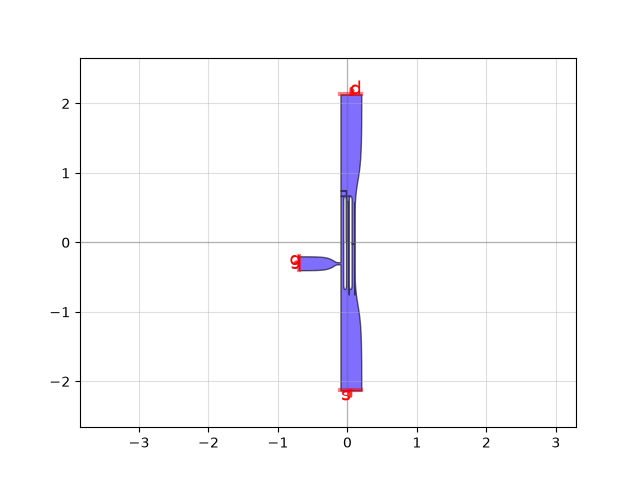
- qnngds.devices.ntron.slotted(base_spec: DeviceSpec = <function smooth>, slot_width: int | float = 0.04, slot_length: int | float = 1.5, slot_pitch: int | float = 0.08, n_slot: int = 2, num_pts: int = 100) Device[source]
Parallel-channel nanocryotron
See [1]
- Parameters:
base_spec (DeviceSpec) – callable function that generates a Device for the base nTron
slot_width (int or float) – width of each slot
slot_length (int or float) – length of each slot
slot_pitch (int or float) – pitch of slots
n_slot (int) – number of slots
num_pts (int) – number of points to use for hairpin
- Returns:
(Device) – nTron with slots
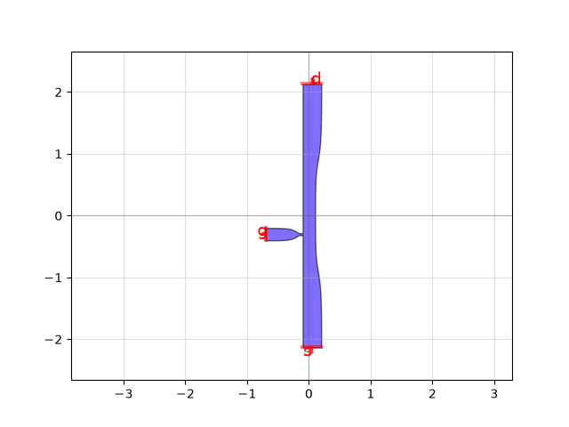
- qnngds.devices.ntron.smooth(choke_w: float = 0.03, gate_w: float = 0.2, channel_w: float = 0.2, source_w: float = 0.3, drain_w: float = 0.3, choke_shift: float = -0.3, num_pts: int = 100, layer: LayerSpec = (1, 0)) Device[source]
Creates a ntron device.
- Parameters:
choke_w (float) – Width of the choke region.
gate_w (float) – Width of the gate region.
channel_w (float) – Width of the channel region.
source_w (float) – Width of the source region.
drain_w (float) – Width of the drain region.
choke_shift (float) – Shift of the choke region.
num_pts (int) – number of points to use for optimal steps
layer (LayerSpec) – GDS layer specification
- Returns:
(Device) – The ntron device.
resistor
Layouts for resistors and resistors with superconducting contacts.
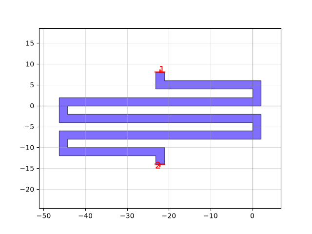
- qnngds.devices.resistor.meander(width: float = 2, pitch: float = 4, squares: float = 100, max_length: float | None = 20, layer: LayerSpec = (1, 0)) Device[source]
Create resistor meander with specified number of squares.
If squares*width > max_length or max_length is None, meander the resistor, destinationwise just return a straight line.
- Parameters:
width (float) – wire width in microns
pitch (float) – desired pitch of meander in microns
squares (float or None) – desired number of squares
max_length (float) – desired length of device
layer (LayerSpec) – GDS layer specification
- Returns:
(Device) – the resistor meander
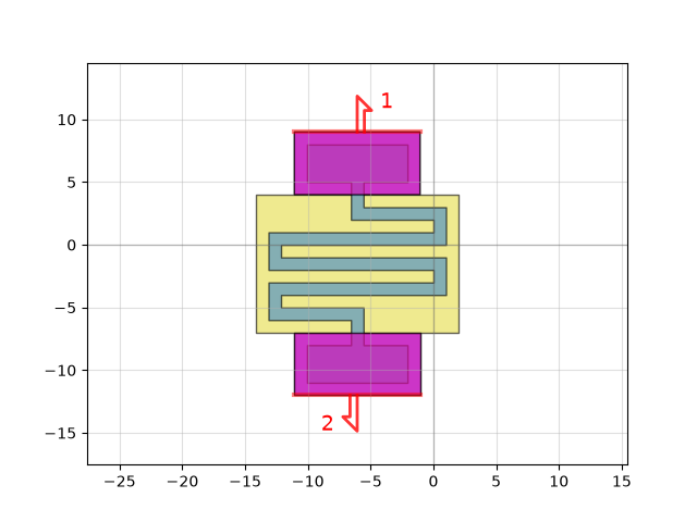
- qnngds.devices.resistor.meander_sc_contacts(width: float = 1, squares: float = 60, max_length: float | None = 10, meander_pitch: float | None = 2, contact_size: tuple[float, float] = (8, 3), outline_contacts: float = 1, layer_res: LayerSpec = 'PHOTO1', layer_contacts: LayerSpecs = ['EBEAM_FINE', 'PHOTO2'], layer_keepout: LayerSpecs = ['EBEAM_KEEPOUT']) Device[source]
Create resistor meander with superconducting contacts.
If squares*width > max_length or if max_length is None, meander the resistor.
- Parameters:
width (float) – width of resistor
squares (float) – desired number of squares
max_length (float or None) – maximum desired length of device
meander_pitch (float or None) – desired pitch of meander in microns
contact_size (tuple[float, float]) – (width, height) of resistor<->superconductor contact
outline_contacts (float) – superconductor extra width on each side of contact
layer_res (LayerSpec) – resistor GDS layer specification
layer_contacts (LayerSpecs) – layer(s) for contact to superconductor (first will define port layer)
layer_keepout (LayerSpecs) – layer(s) to do keepout on
- Returns:
(Device) – the resistor meander
resonator
Layout for various superconducting resonators.
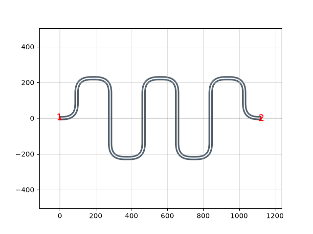
- qnngds.devices.resonator.meandered(cross_section: CrossSectionSpec = <function cpw>, n_eff: float = 10, resonant_freq: float = 5000000000.0, meander_width: float = 500) Device[source]
Construct meandered half-wave resonator
- Parameters:
n_eff (float) – effective index of refraction
resonant_freq (float) – resonant frequeny in Hz
meander_width (float) – width of meander structure
cross_section (CrossSectionSpec) – cross section to use (e.g. CPW)
- Returns:
(Device) – meandered half-wave resonator
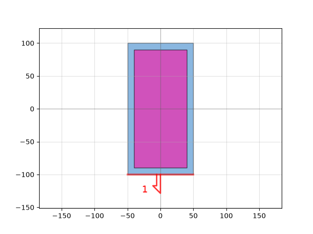
- qnngds.devices.resonator.pad(width: float = 100, length: float = 200, edge_exclusion: float = 10, sc_layer: LayerSpec = 'PHOTO1', metal_layers: LayerSpecs = ('PHOTO2',)) Device[source]
Construct a pad for resonator with a metal layer for bonding on top of superconductor.
- Parameters:
width (float) – Desired width of superconductor layer
edge_exclusion (float) – Amount on each side to decrease width of top metal bonding pad.
sc_layer (LayerSpec) – layer specification for superconductor
metal_layers (LayerSpecs) – layer(s) for metal
- Returns:
(Device) – pad
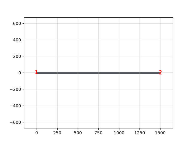
- qnngds.devices.resonator.straight(cross_section: CrossSectionSpec = <function cpw>, n_eff: float = 100, resonant_freq: float = 1000000000.0) Device[source]
Construct straight half-wave resonator
- Parameters:
cross_section (CrossSectionSpec) – cross section to use (e.g. CPW)
n_eff (float) – effective index of refraction
resonant_freq (float) – resonant frequeny in Hz
- Returns:
(Device) – meandered half-wave resonator
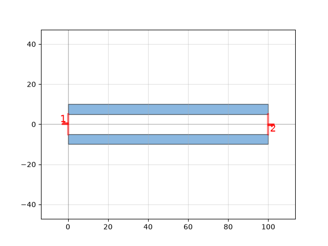
- qnngds.devices.resonator.transmission_line(cross_section: CrossSectionSpec = <function cpw>, length: float = 100) Device[source]
Construct a straight transmission line by extruding a cross section
- Parameters:
length (float) – length of transmission line
cross_section (CrossSectionSpec) – cross section to extrude
- Returns:
(Device) – straight transmission line
- qnngds.devices.resonator.transmission_line_resonator(transmission_line_specs: tuple[DeviceSpec | None, DeviceSpec | None] = (<function transmission_line>, None), resonator_spec: DeviceSpec = <function meandered>, tl_cross_section: CrossSectionSpec = functools.partial(<function cpw>, width=75, gap=24), res_cross_section: CrossSectionSpec = <function cpw>, taper: DeviceFactory = <function hyper_taper>, pads: tuple[DeviceSpec | None, DeviceSpec | None] = (<function pad>, None), bbox_extension: float = 500) Device[source]
Construct a resonator embedded between two transmission lines
Inverts final design based on layer choice and PDK Layer class’s outline function
- Parameters:
transmission_line_specs (tuple[DeviceSpec | None, DeviceSpec | None]) – Desired DeviceSpec for transmission line on either end of resonator. If DeviceSpec, take a single argument
cross_section. If None, no transmission line will be created (although the resonator will taper out to the width of thetl_cross_section.resonator_spec (DeviceSpec) – Desired DeviceSpec for embedded resonator. Must take a single argument
cross_section.tl_cross_section (CrossSectionSpec) – CPW or microstrip cross section for transmission line.
res_cross_section (CrossSectionSpec) – CPW or microstrip cross section for resonator.
taper (DeviceFactory) – Callable which produces a Device, used to generate a filled taper between resonator and transmission line. Port widths must match. Should be solid (i.e. not outlined); will be automatically outlined for CPW.
pads (tuple[DeviceSpec | None, DeviceSpec | None]) – DeviceSpec or None for each pad. If DeviceSpec, must take a single argument
width. If None, no pad will be createdbbox_extension (float) – amount to extend ground plane for negative tone layout CPW, or positive tone microstrip
- Returns:
(Device) – resonator embedded between transmission lines
Example:
>>> from functools import partial
>>> tl_spec = partial(
>>>     qg.devices.resonator.transmission_line,
>>>     length=100,
>>> )
>>> res_spec = partial(
>>>     qg.devices.resonator.meandered,
>>>     n_eff=100,
>>>     resonant_freq=1e9,
>>>     meander_width=300,
>>> )
>>> tl_xc_spec = partial(
>>>     qg.devices.resonator.cpw,
>>>     width=20,
>>>     gap=4,
>>>     layer="PHOTO1",
>>> )
>>> res_xc_spec = partial(
>>>     qg.devices.resonator.cpw,
>>>     width=10,
>>>     radius=30,
>>>     gap=2,
>>>     layer="PHOTO1",
>>> )
>>> c = qg.devices.resonator.transmission_line_resonator(
>>>     transmission_line_specs=(tl_spec, None),
>>>     resonator_spec=res_spec,
>>>     tl_cross_section=tl_xc_spec,
>>>     res_cross_section=res_xc_spec,
>>>     taper=qg.geometries.hyper_taper,
>>>     pads=(qg.devices.resonator.pad, None),
>>>     bbox_extension=200,
>>> )
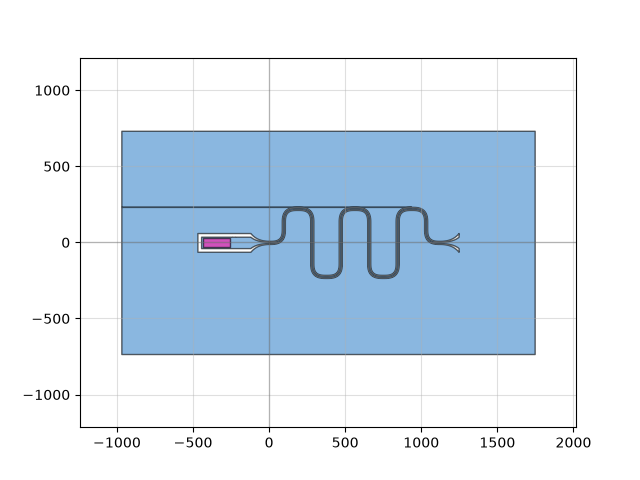
- qnngds.devices.resonator.compute_veff(n_eff: float) float[source]
Computes effective light speed from effective index
- Parameters:
n_eff – effective index of refraction
- Returns:
(float) – effective phase velocity in m/s
- qnngds.devices.resonator.compute_res_wavelength(n_eff: float, res_freq: float) float[source]
Computes resonant wavelength from effective index, resonant frequency.
- Parameters:
n_eff – effective index of refraction
res_freq – resonant frequency in Hz
- Returns:
(float) – resonant wavelength in microns
- qnngds.devices.resonator.cpw(width: float = 10, gap: float = 5, radius: float = 50, layer: LayerSpec = 'PHOTO1') CrossSection[source]
Creates a coplanar waveguide (CPW) cross section.
NB resulting cross section is inverted: gaps will be filled and conductor will be empty.
- Parameters:
width (float) – width of center conductor
gap (float) – width of gaps on either side of conductor
radius (float) – bend radius
layer (LayerSpec) – GDS layer specification
- Returns:
(CrossSection) – CPW cross section
- qnngds.devices.resonator.microstrip(width: float = 5, radius: float = 50, layer: LayerSpec = 'PHOTO1') CrossSection[source]
Creates a microstrip cross section
NB unlike
cpw(), conductor is filled- Parameters:
width (float) – width of center conductor
radius (float) – bend radius
layer (LayerSpec) – GDS layer specification
- Returns:
(CrossSection) – microstrip cross section
snspd
Superconducting nanowire single photon detector geometries.
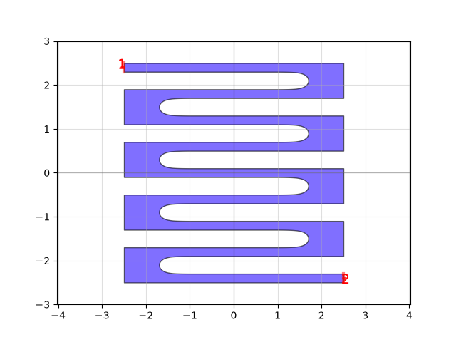
- qnngds.devices.snspd.basic(wire_width: float = 0.2, wire_pitch: float = 0.6, size: Tuple[int | float | None, int | float | None] = (5, 5), num_squares: int | None = None, turn_ratio: int | float = 4, num_pts: int = 50, extend_terminals: bool = True, terminals_same_side: bool = False, layer: LayerSpec = (1, 0)) Device[source]
Creates an optimally-rounded SNSPD.
Modification of gdsfactory’s and phidl’s implementations
- Parameters:
wire_width (float) – Width of the nanowire.
wire_pitch (float) – Pitch of the nanowire.
size (tuple of Optional[int or float]) – Size of the detector.
num_squares (int | None) – Number of squares in the detector.
turn_ratio (int or float) – Specifies how much of the SNSPD width is dedicated to the 180 degree turn. A turn_ratio of 10 will result in 20% of the width being comprised of the turn.
num_pts (int) – number of polygon points to use for turn
extend_terminals (bool) – If True, bring ports flush to edges of device also allows shorter device by overlapping hairpins.
terminals_same_side (bool) – If True, both ports will be located on the same side of the SNSPD.
layer (LayerSpec) – GDS layer specification
- Returns:
(Device) – optimally-rounded SNSPD, as provided by Phidl but renamed and unified.
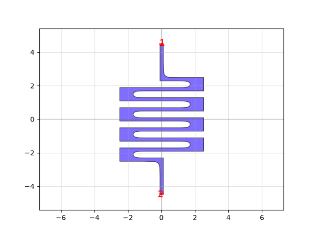
- qnngds.devices.snspd.vertical(wire_width: float = 0.2, wire_pitch: float = 0.6, size: Tuple[int | float, int | float] = (5, 5), num_squares: int | None = None, extend: float | None = 1, num_pts: int = 50, layer: LayerSpec = (1, 0)) Device[source]
Creates an optimally-rounded SNSPD, with terminals in its center instead of the side.
- Parameters:
wire_width (float) – Width of the nanowire.
wire_pitch (float) – Pitch of the nanowire.
size (tuple of int or float) – Size of the detector.
num_squares (int | None) – Number of squares in the detector.
extend (bool | None) – Whether or not to extend the ports.
num_pts (int) – number of points to use for optimal hairpin.
layer (LayerSpec) – GDS layer specification
- Returns:
(Device) – The vertical SNSPD device.
experiment
Utilities for generating experiments from devices or circuits, automatically routing between device/circuit and pads and performing outlining and boolean keepout operations based on PDK requirements.
- class qnngds.experiment.RouteGroup(cross_section: CrossSectionSpec, port_mapping: dict | tuple, ground: bool = False)[source]
Bases:
objectStores information for routing DUTs to pads.
Stores a cross section and mapping of DUT ports to optional pad ports. If a DUT port is mapped to None, then a pad port will be automatically assigned in
generate()- __init__(cross_section: CrossSectionSpec, port_mapping: dict | tuple, ground: bool = False)[source]
Initialize route group
- Parameters:
cross_section (CrossSectionSpec) – factory method for desired cross section used for routing
port_mapping (dict | tuple) – either dictionary manually specifying mapping of DUT port names to pad port names or a tuple of DUT port names that should be mapped automatically to pad ports.
ground (bool) – If True, then all dut ports will not be connected to a pad port. This allows connection to ground plane for positive-tone layouts.
- Returns:
None
- qnngds.experiment.generate(dut: DeviceSpec | Device, pad_array: DeviceSpec | Device, label: DeviceSpec | Device | None, route_groups: Sequence[RouteGroup], dut_offset: tuple[float, float] = (0, 0), pad_offset: tuple[float, float] = (0, 0), label_offset: tuple[float, float] | None = (-100, -100), ignore_port_count_mismatch: bool = False, ignore_dut_bbox: bool = False, retries: int = 10, debug: bool = False) Device[source]
Construct an experiment from a device/circuit (Device).
Includes text, pads, and routing to connect pads to devices
- Parameters:
dut (DeviceSpec or Device) – finished device to be connected to pads
pad_array (DeviceSpec or Device or None) – pad array to connect to device
label (DeviceSpec or Device or None) – text label or factory.
route_groups (Sequence[RouteGroup]) – how to route DUT to pads
dut_offset (tuple[float, float]) – x,y offset for dut (mostly useful for linear pad arrays)
pad_offset (tuple[float, float]) – x,y offset for pad array (mostly useful for linear pad arrays)
label_offset (tuple[float, float] or None) – x,y offset of label
ignore_port_count_mismatch (bool) – if True, ignores mismatched number of DUT and pads ports, only if route_groups defines a mapping to all pad ports, or lists all DUT ports.
ignore_dut_bbox (bool) – if True, does not attempt to route around DUT bounding box (bbox)
retries (int) – how many times to try rerouting with s_bend (may need to be larger for many port groupings)
debug (bool) – if True, quickplot DUT + pads before throwing error when routing fails
- Returns:
(Device) – experiment
Example
Using the example qnngds PDK: https://github.com/qnngroup/qnngds-pdk/, we can generate an example nTron test layout including pads. The pad array is just a linear array from gdsfactory, although a custom array could be defined. The mapping of nTron device ports to pad ports is defined manually with
route_groups, but it’s possible to use autoassignment by settingroute_groups=None. However, autoassignment only works in some cases, and in the case of this nTron, it would most likely fail.>>> c = qg.experiment.generate( >>> dut=qg.devices.ntron.sharp, >>> pad_array=qg.pads.array( >>> pad_specs=(qg.pads.stack(size=(200, 200), layers=("EBEAM_COARSE",)),), >>> columns=1, >>> rows=3, >>> pitch=250, >>> ), >>> label=None, >>> route_groups=( >>> qg.experiment.RouteGroup( >>> qg.get_cross_section("ebeam"), {"g": 2, "s": 1, "d": 3} >>> ), >>> ), >>> dut_offset=(250, 250), >>> pad_offset=(0, 0), >>> label_offset=(0, 0), >>> retries=1, >>> ) >>> qp(c)
geometries
Geometries contains useful shapes/tools that are not available in phidl’s geometry library.
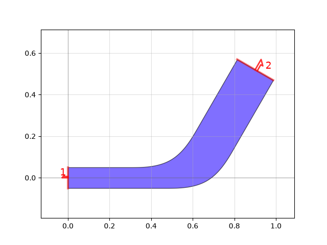
- qnngds.geometries.angled_taper(end_width: int | float = 0.2, start_width: int | float = 0.1, angle: int | float = 60, layer: LayerSpec = (1, 0)) Device[source]
Create an angled taper with euler curves.
- Parameters:
end_width (int or float) – Width of wide end of taper
start_width (int or float) – Width of narrow end of taper
angle (int or float) – Angle between taper ends in degrees
layer (LayerSpec) – GDS layer specification
- Returns:
(Device) – a single taper
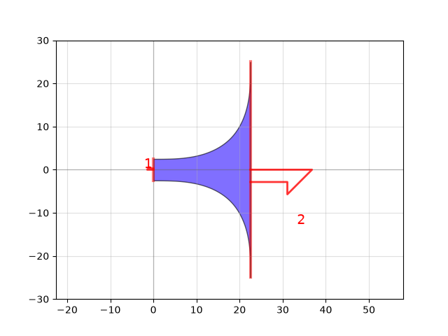
- qnngds.geometries.euler_taper(start_width: int | float = 5, end_width: int | float = 50, layer: LayerSpec = (1, 0), num_points: int = 200) Device[source]
Euler taper (solid). Designed by reedf.
- Parameters:
length (int | float) – Length of taper
start_width (int | float) – Width of start of taper
end_width (int | float) – Width of end of taper
layer (LayerSpec) – GDS layer specification
num_points (int) – number of points to use
- Returns:
(Device) – a single taper
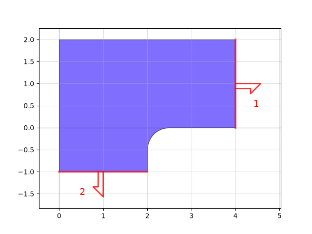
- qnngds.geometries.fillet_90deg(size: tuple[float, float] = (4, 2), stub_size: tuple[float, float] = (2, 1), taper_type: str | None = 'fillet', taper_radius: float | None = None, layer: LayerSpec = (1, 0)) Device[source]
Creates a 90 degree with fillet bend. Adapted from phidl.flagpole
- Parameters:
size (array-like) – (width, height) of the flag.
stub_size – (array-like): (width, height) of the pole stub.
taper_type (str | None) – {‘straight’, ‘fillet’, None} Type of taper between the bottom corner of the stub on the side of the flag and the corner of the flag closest to the stub.
taper_radius (float | None) – radius of taper. If None, uses stub_size
layer (LayerSpec) – Specification of layer(s) to put polygon geometry on.
- Returns:
(Device) – fillet_90deg
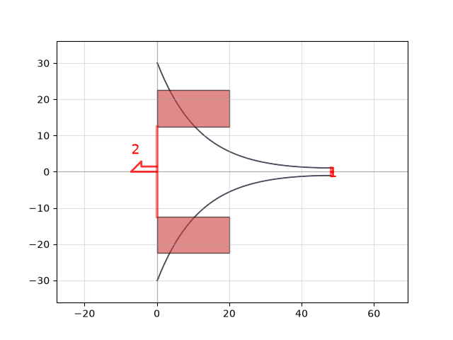
- qnngds.geometries.fine_to_coarse(width1: float = 2.0, width2: float = 20.0, layer1: LayerSpec = 'EBEAM_FINE', layer2: LayerSpec = 'EBEAM_COARSE') Device[source]
Create transition between fine and coarse layers.
Automatically performs outlining for positive-tone resist.
- Parameters:
width1 (float) – starting width on first layer
width2 (float) – ending width on second layer
layer1 (LayerSpec) – layer specification for first layer
layer2 (LayerSpec) – layer specification for second layer
- Returns:
(Device) – transition between fine and coarse layers
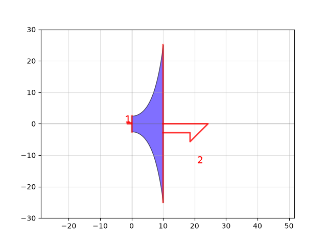
- qnngds.geometries.hyper_taper(length: int | float = 10, start_width: int | float = 5, end_width: int | float = 50, layer: LayerSpec = (1, 0), num_points: int = 50) Device[source]
Hyperbolic taper (solid). Designed by colang.
- Parameters:
length (int or float) – Length of taper
start_width (int or float) – Width of start of taper
end_width (int or float) – Width of end of taper
layer (LayerSpec) – GDS layer specification
num_points (int) – number of points to use
- Returns:
(Device) – a single taper
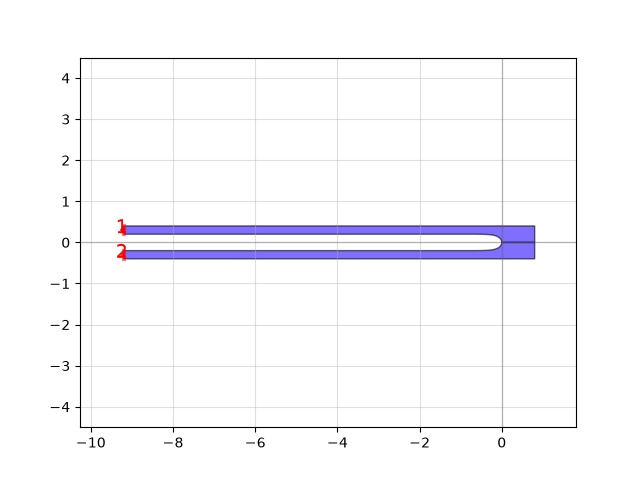
- qnngds.geometries.optimal_hairpin(width: float | int = 0.2, pitch: float | int = 0.6, length: float | int = 10, turn_ratio: float | int = 4, num_pts: float | int = 50, layer: LayerSpec = (1, 0)) qg.Device[source]
Returns an optimally-rounded hairpin geometry, with a 180 degree turn.
based on phidl.geometry. Used instead of phidl implementation to center the apex of the hairpin at (0, 0).
- Parameters:
width – Width of the hairpin leads.
pitch – Distance between the two hairpin leads. Must be greater than width.
length – Length of the hairpin from the connectors to the opposite end of the curve.
turn_ratio – int or float Specifies how much of the hairpin is dedicated to the 180 degree turn. A turn_ratio of 10 will result in 20% of the hairpin being comprised of the turn.
num_pts – Number of points constituting the 180 degree turn.
layer – Specific layer(s) to put polygon geometry on.
Notes
Hairpin pitch must be greater than width.
Optimal structure from https://doi.org/10.1103/PhysRevB.84.174510 Clem, J., & Berggren, K. (2011). Geometry-dependent critical currents in superconducting nanocircuits. Physical Review B, 84(17), 1-27.
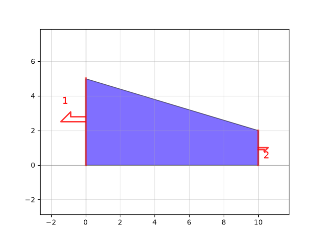
- qnngds.geometries.ramp(length: int | float = 10, start_width: int | float = 5, end_width: int | float = 2, layer: LayerSpec = (1, 0)) Device[source]
Linear ramp (solid). Asymmetric version of taper.
- Parameters:
length (int or float) – Length of ramp
start_width (int or float) – Width of first end of ramp
end_width (int or float) – Width of second end of ramp
layer (LayerSpec) – GDS layer specification
- Returns:
(Device) – a single taper
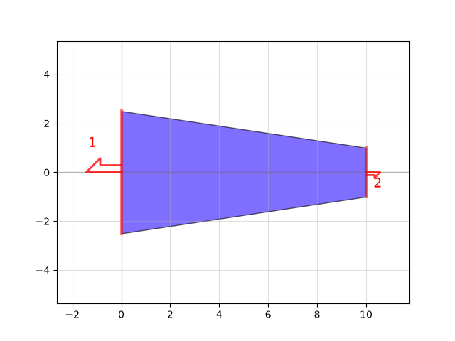
- qnngds.geometries.taper(length: int | float = 10, start_width: int | float = 5, end_width: int | float = 2, layer: LayerSpec = (1, 0)) Device[source]
Linear taper (solid).
- Parameters:
length (int or float) – Length of taper
start_width (int or float) – Width of first end of taper
end_width (int or float) – Width of second end of taper
layer (LayerSpec) – GDS layer specification
- Returns:
(Device) – a single taper
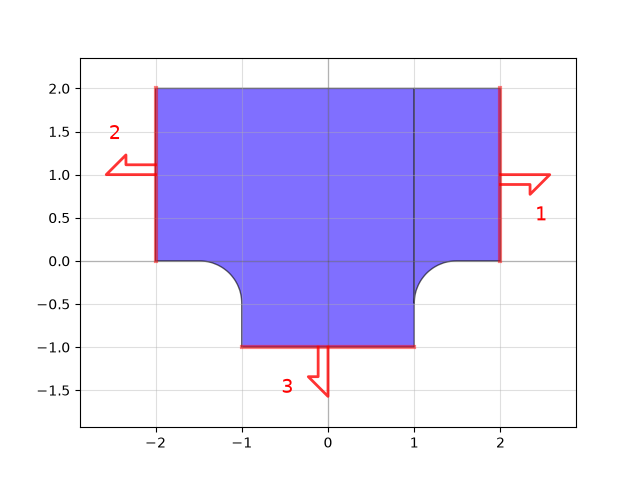
- qnngds.geometries.tee(size: tuple[float, float] = (4, 2), stub_size: tuple[float, float] = (2, 1), taper_type: str | None = 'fillet', taper_radius: float | None = None, layer: LayerSpec = (1, 0)) Device[source]
Creates a T-shaped geometry.
Adapted from phidl and adds additional argument to specify the radius of fillet tapers.
- Parameters:
size (array-like) – (width, height) of the tee.
stub_size – (array-like): (width, height) of the stub.
taper_type (str | None) – {‘straight’, ‘fillet’, None} Type of taper between the bottom corner of the stub on the side of the flag and the corner of the flag closest to the stub.
taper_radius (float | None) – radius of taper. If None, uses stub_size
layer (LayerSpec) – Specification of layer(s) to put polygon geometry on.
- Returns:
(Device) – tee
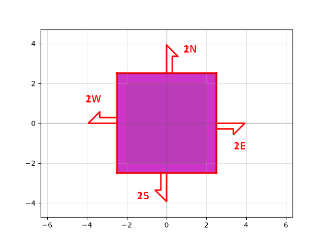
- qnngds.geometries.via(size: tuple[float, float] = (5, 5), via_undersize: float = 0.5, layer_bottom: LayerSpec = (1, 0), layer_via: LayerSpec = (10, 0), layer_top: LayerSpec = (20, 0)) Device[source]
Creates a via between two layers
- Parameters:
size (tuple[float, float]) – width, height of top/bottom pads
via_undersize (float) – amount on each side to compensate overetch of via
layer_bottom (LayerSpec) – bottom layer specification
layer_via (LayerSpec) – via layer specification
layer_top (LayerSpec) – top layer specification
- Returns:
(Device) – via
- qnngds.geometries.default_cross_section(width: float = 25, layer: LayerSpec = (1, 0), radius: float = 30.0, force_no_outline: bool = False) CrossSection[source]
Return a default cross_section.
- Parameters:
width (float) – width of cross section
layer (LayerSpec) – layer specification for cross section
radius (float) – bend radius
force_no_outline (bool) – if True, ignores if layer is positive tone.
- Returns:
(CrossSection)
layout
Extend phidl’s Layout classes:
- Modifications:
Port: add layer information
CellArray: add ports
Layer: add outline/keepout info
CrossSection: allow “hidden” sections
- class qnngds.layout.Port(name: str = None, midpoint: ArrayLike = (0, 0), width: float = 1, orientation: float = 0, layer: LayerSpec = (1, 0), parent=None)[source]
Bases:
PortPort object used to snap objects together. Extends phidl.Port to add layer information
- __init__(name: str = None, midpoint: ArrayLike = (0, 0), width: float = 1, orientation: float = 0, layer: LayerSpec = (1, 0), parent=None) None[source]
Constructor for Port.
- Parameters:
name (str) – name of port
midpoint (np.ArrayLike) – midpoint of port location
width (float) – width of float
orientation (float) – rotation of port
layer (LayerSpec) – GDS layer specification
parent
- class qnngds.layout.Device(*args, **kwargs)[source]
Bases:
DeviceThe basic object that holds polygons, labels, and ports in PHIDL. Augmented with methods for layer-assigned ports.
- add_port(name: str = None, midpoint: ArrayLike = (0, 0), width: float = 1, orientation: float = 0, layer: LayerSpec = None, port: Port | None = None) Port[source]
Adds a Port to the Device.
- Parameters:
name (str) – name of port
midpoint (tuple[float,float]) – midpoint of port location
width (float) – width of float
orientation (float) – rotation of port
layer (LayerSpec) – GDS layer specification
port (Port | None) – a Port if the added Port is a copy of an existing Port.
Notes
Can be called to copy an existing port like
add_port(port = existing_port)or to create a new portadd_port(myname, mymidpoint, mywidth, myorientation, mylayer). Can also be called to copy an existing port with a new name likeadd_port(port = existing_port, name = new_name)- Returns:
(Port) – created port
- add_ports(ports: Sequence[Port]) None[source]
Add multiple Ports to Device
- Parameters:
ports (Sequence[Port]) – multiple Port objects to be added
- add_array(device: Device, columns: int = 2, rows: int = 2, spacing: tuple[float, float] = (100, 100), alias: str | None = None) DeviceArray[source]
Creates a DeviceArray reference.
- Parameters:
device (Device) – the referenced Device.
columns (int) – number of columns in the array.
rows (int) – number of rows in the array.
spacing (Arraylike) – (column spacing, row spacing)
alias (str | None) – Alias of the referenced Device.
- Returns:
(DeviceArray) – array containing references to the input Device.
- name
- polygons
- paths
- labels
- references
- class qnngds.layout.DeviceArray(*args, **kwargs)[source]
Bases:
CellArrayAugmentation of gdspy/phidl’s CellArray class, autogenerates a port dictionary for all instances
- __init__(*args, **kwargs) None[source]
Calls PHIDL constructor for CellArray, then generates ports for each reference in array
- columns
- rows
- rotate(angle=45, center=(0, 0)) None[source]
Rotate underlying CellArray and update ports
- Parameters:
angle (float) – rotation angle
center (Arraylike) – coordinates about which to perform rotation
- move(origin=(0, 0), destination=None, axis=None) None[source]
Translate underlying CellArray and update ports
- Parameters:
origin (tuple) – starting location
destination (Arraylike | None) – destination
axis
- ref_cell
- origin
- rotation
- magnification
- x_reflection
- spacing
- properties
- class qnngds.layout.Layer(gds_layer: int = 0, gds_datatype: int = 0, name: str = 'unnamed', description: str | bool = None, inverted: bool = False, color: str | tuple | None = None, alpha: int | float = 0.6, dither: str | None = None, keepout: LayerSpecs | Sequence[Layer] | None = None, outline: int | float = 0)[source]
Bases:
LayerAugment PHIDL Layer with outline and keepout information
- __init__(gds_layer: int = 0, gds_datatype: int = 0, name: str = 'unnamed', description: str | bool = None, inverted: bool = False, color: str | tuple | None = None, alpha: int | float = 0.6, dither: str | None = None, keepout: LayerSpecs | Sequence[Layer] | None = None, outline: int | float = 0) None[source]
Constructor for qnngds.Layer
- Parameters:
keepout (LayerSpecs | Layers | None) – if not None, defines one or more Layers for which the current layer defines keepout regions.
outline (int | float) – if non-zero, makes layer positive tone, written with a linewidth of outline.
- class qnngds.layout.LayerSet[source]
Bases:
LayerSetAugment PHIDL LayerSet to use Layers with outline and keepout information
- class qnngds.layout.CrossSection(radius: int | float = 0)[source]
Bases:
CrossSectionAugment PHIDL CrossSection to allow for hidden layers and radius specification
- __init__(radius: int | float = 0) None[source]
Constructor for CrossSection
- Parameters:
radius (float | int) – nominal radius used when autogenerating paths. NB explicitly providing a radius (e.g. when manually creating paths) will override this setting
- add(width: float | int = 1, offset: float | int = 0, layer: int | tuple[int, int] = 0, ports: tuple[int | str | None] = (None, None), name: str | None = None, hidden: bool = False, min_radius: float | int = 0) CrossSection[source]
Calls phidl.CrossSection.add() method, and also updates hidden variable
- Parameters:
width (float | int | callable) – Width of the segment
offset (float | int | callable) – Offset of the segment (positive values = right hand side)
layer (int | tuple[int, int]) – The polygon layer to put the segment on
ports (array-like[2] of str | int | None) – If not None, specifies the names for the ports at the ends of the cross-sectional element.
name (str | int | None) – Name of the cross-sectional element for later access
hidden (bool) – if True, does not add polygon during extrusion
- Returns:
(CrossSection) – updated self
pads
Pads contains functions for generation of pads and pad arrays.
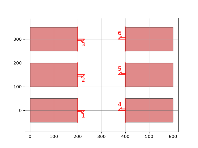
- qnngds.pads.array_dual(array_spec: DeviceSpec = <function array_single>, space: float = 200) Device[source]
Creates dual linear arrays of pads that face each other
- Parameters:
array_spec (DeviceSpec) – specification for a single array
space (float) – distance between pad ports for each array
- Returns:
(Device) – dual linear pad array
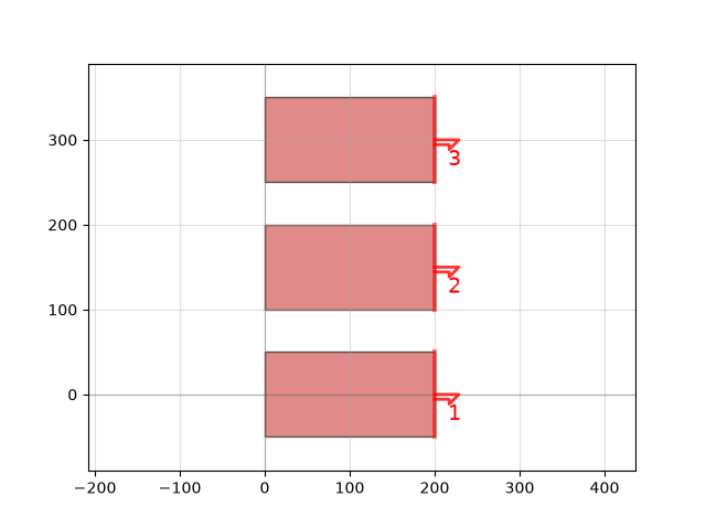
- qnngds.pads.array_single(pad_specs: DeviceSpecs = (<function stack>, ), columns: int = 1, rows: int = 3, pitch: float = 150) Device[source]
Creates a single linear array of pads
- Parameters:
pad_spec (DeviceSpec) – specification for pad or pad stack to use
columns (int) – number of columns
rows (int) – number of rows
pitch (float) – pitch of pads (same for rows/columns)
- Returns:
(Device) – linear pad array
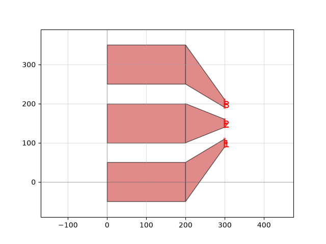
- qnngds.pads.quad_line(array_spec: DeviceSpec = <function array_single>, port_width: float = 20, port_pitch: float = 50, port_offset: tuple[float, float] = (100, 0)) Device[source]
Create pads with quad routing to intermediate ports
- Parameters:
array_spec (DeviceSpec) – spec for pad array (assumes 1D array along y-axis)
port_width (float) – width of intermediate ports
port_pitch (float) – pitch of intermediate ports
port_offset (tuple[float, float]) – offset of intermediate ports relative to pad array port center
- Returns:
(Device) – pads with intermediate finer ports
- qnngds.pads.stack(size: tuple[float, float] = (200, 100), layers: LayerSpecs = ('EBEAM_COARSE',), port_span: tuple[float, float] = (0, 1)) Device[source]
Create pad stack for use in other pad arrays
Has a single port facing to the right
- Parameters:
size (tuple[float, float]) – width, height of pad
layers (LayerSpecs) – One or more layers to stack. First layer will have a port, which is the layer that will be used for routing to the pad.
port_span (tuple[float, float]) – fraction on [0,1] for starting and ending point of port
- Returns:
(Device) – pad stack
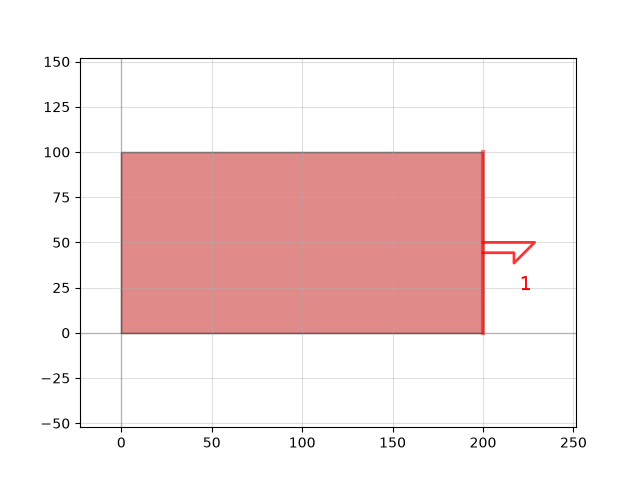
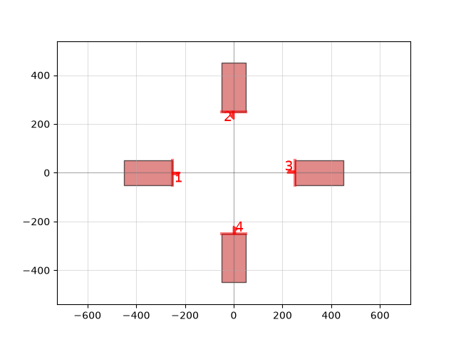
- qnngds.pads.vdp(pad_specs: DeviceSpecs = (<function stack>, ), space: float = 500) Device[source]
Create pads for Van der Pauw probing
- Parameters:
pad_specs (DeviceSpecs) – specification for pad or pad stack to use. Can be a single element tuple or 4 different pads.
space (float) – Spacing between pads (diagonal of VDP cell)
- Returns:
(Device) – Van der Pauw pad structure
pdk
Pdk functions for layer and device management, mostly taken from gdsfactory
- class qnngds.pdk.Pdk(name: str, layers: LayerSet, cross_sections: dict[str, CrossSection] = {}, layer_transitions: dict[LayerSpec | tuple[LayerSpec, LayerSpec], DeviceSpec] = {}, devices: DeviceSpecs = [])[source]
Bases:
objectPDK class, stores layer information, cross sections, layer transistions, and devices
- __init__(name: str, layers: LayerSet, cross_sections: dict[str, CrossSection] = {}, layer_transitions: dict[LayerSpec | tuple[LayerSpec, LayerSpec], DeviceSpec] = {}, devices: DeviceSpecs = []) None[source]
Constructor
- Parameters:
name (str) – name of PDK
layers (LayerSet) – LayerSet to use for PDK
cross_sections (dict[str, CrossSection]) – map of named cross sections to their instances.
layer_transitions (dict[LayerSpec | tuple[LayerSpec, LayerSpec], DeviceSpec]) – map of LayerSpec (or pair of LayerSpecs) to a DeviceSpec which will transition between layers.
devices (DeviceSpecs) – devices to register with PDK
- Returns:
None
- get_layer(layer: LayerSpec) Layer[source]
Get a specific layer within the PDK
- Parameters:
layer (LayerSpec) – string, int, or tuple that identifies the desired layer
- Returns:
(Layer) – instance of layer matching the queried LayerSpec
- get_device(spec: DeviceSpec, **kwargs: dict) phidl.Device[source]
Get a specific device within the PDK
- Parameters:
spec (DeviceSpec) – device instance, name (string), or callable function that identifies desired device
kwargs (dict) – keyword arguments to pass to spec.
- Returns:
(Device) – instance of device matching the queried DeviceSpec
- get_cross_section(spec: CrossSectionSpec) phidl.CrossSection[source]
Get a specific layer within the PDK
- Parameters:
spec (CrossSectionSpec) – device instance, name (string), or callable function that identifies desired device
- Returns:
(CrossSection) – instance of device matching the queried CrossSectionSpec
- qnngds.pdk.get_generic_pdk() Pdk[source]
Get a generic PDK
Includes the following layers: * EBEAM_FINE (1, 0), outline=0.1 * EBEAM_COARSE (2, 0), outline=10 * EBEAM_KEEPOUT (3, 0), keepout=(EBEAM_FINE,) * PHOTO1 (10, 0) * PHOTO2 (20, 0) * PHOTO3 (30, 0) * PHOTO4 (40, 0)
Includes the following cross-sections for routing: * ebeam (EBEAM_COARSE) * photo1 (PHOTO1) * photo2 (PHOTO2) * photo3 (PHOTO3) * photo4 (PHOTO4)
Includes the following layer transitions: * EBEAM_FINE <-> EBEAM_COARSE * all transitions within the same layer
- qnngds.pdk.get_layer(layer: LayerSpec) Layer[source]
Get a specific layer within the globally-activated PDK
- Parameters:
layer (LayerSpec) – string, int, or tuple that identifies the desired layer
- Returns:
(Layer) – instance of layer matching the queried LayerSpec
- qnngds.pdk.get_device(spec: DeviceSpec, **kwargs: dict) phidl.Device[source]
Get a specific layer within the globally-activated PDK
- Parameters:
spec (DeviceSpec) – device instance, name (string), or callable function that identifies desired device
kwargs (dict) – Keyword arguments to pass to spec.
- Returns:
(Device) – instance of device matching the queried DeviceSpec
- qnngds.pdk.get_cross_section(cross_section: CrossSectionSpec) phidl.CrossSection[source]
Get a specific layer within the globally-activated PDK
- Parameters:
cross_section (CrossSectionSpec) – cross_section instance, name (string), or callable function that identifies desired cross_section
- Returns:
(CrossSection) – instance of cross_section matching the queried CrossSectionSpec
- qnngds.pdk.layer_auto_transitions(layer_set: LayerSet) dict[LayerSpec, DeviceSpec][source]
Generate layer_transitions dictionary for auto tapers within the same layer
- Parameters:
layer_set (LayerSet) – layers in PDK for which the auto transitions should be generated
- Returns:
(dict[Layer, DeviceSpec]) – mapping the appropriate taper for each layer auto transitions
sample
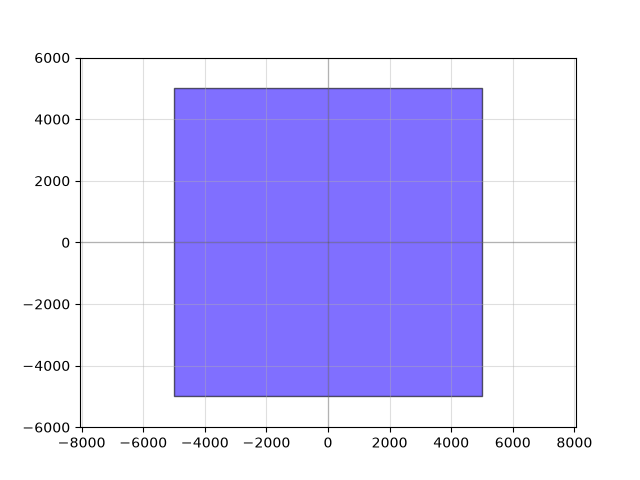
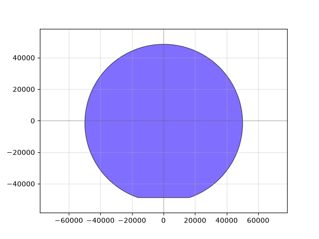
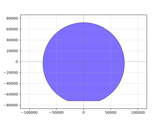
Sample defines the Sample class which is used to generate a wafer/piece layout from multiple experiments
- exception qnngds.sample.PlaceError(message)[source]
Bases:
ExceptionException raised when placement fails
- class qnngds.sample.Sample(cell_size: float = 10000, sample: DeviceSpec | Device = <function wafer100mm>, edge_exclusion: float = 10000, allow_cell_span: bool = False)[source]
Bases:
objectClass for managing die/experiment area, with manual placement and basic autoplacement
Defines a grid size and divides a sample (wafer/piece) into cells. Experiments (generated with
qnngds.utilities.generate_experiment()) can be placed on one or more cells in the grid, manually or automatically. If initialized withallow_cell_span, experiments can span multiple columns/rows.For a wafer, it is recommended to have two hierarchies of
Samples. At the top-level, define a wafer-sized Sample, with a number of cells that can be cut/cleaved into dies. Each cell may be defined as aSampleto place multiple experiments on a grid within the die. For example:>>> my_experiment_die_1 = qg.sample.Sample( >>> cell_size=1e3, sample=qg.sample.piece10mm, edge_exclusion=500, allow_cell_span=True, >>> ) >>> # place experiments (e.g. circuits, devices, lithographic structures etc.) on nTron_die >>> # ... >>> # create other dies >>> # ... >>> # ... >>> sample = qg.sample.Sample( >>> cell_size=10e3, sample=qg.sample.wafer100mm, edge_exclusion=10e3, allow_cell_span=False, >>> ) >>> # place nTron_die and other dies on sample
- __init__(cell_size: float = 10000, sample: DeviceSpec | Device = <function wafer100mm>, edge_exclusion: float = 10000, allow_cell_span: bool = False) None[source]
Constructor for Sample class
- Parameters:
cell_size (float) – pitch of cell grid
sample (Device | DeviceSpec) – desired sample shape (e.g. wafer/piece)
edge_exclusion (float) – desired edge exclusion for die placement
allow_cell_span (bool) – if True, allows a device added to the sample to span multiple cells
- Returns:
None
- visualize_open_cells() Device[source]
Visualize open cells
- Returns:
(Device) – device used for visualization
- place_on_sample(device: Device, cell_coordinate_bbox: tuple, ignore_collisions: bool = False) None[source]
Place device on sample
See also
place_multiple_on_sample().- Parameters:
device (Device) – device to place
cell_coordinate_bbox (tuple[int, int] | tuple[tuple[int, int], tuple[int, int]]) – bounding box of cell coordiantes within which the device should be placed. If the device fits within a single cell, then a tuple[int, int] is acceptable instead of passing a tuple with identical coordinates for the bbox. If device spans multiple cells, then the bbox coordinates must be unique.
ignore_collisions (bool) – If True, ignores any collision of device with previously-placed devices.
- Returns:
None
- Side Effects:
Updates self.open_cells to remove newly allocated cells Updates self.full_cells to add newly allocated cells
- place_multiple_on_sample(devices: Sequence[Device], cell_coordinate_bbox: tuple, column_major: bool = True, ignore_collisions: bool = False) None[source]
Place devices on sample
See also
place_on_sample().- Parameters:
devices (Sequence[Device]) – sequence of devices to place
cell_coordinate_bbox (tuple[tuple[int, int], tuple[int, int]]) – bounding box of cell coordiantes within which the device should be placed.
column_major (bool) – If True, orders devices in column-major order within bbox. (top-to-bottom, then left-to-right). Otherwise, orders row-major (left-to-right, then top-to-bottom).
ignore_collisions (bool) – If True, ignores any collision of device with previously-placed devices.
- Returns:
None
- Side Effects:
Updates self.open_cells to remove newly allocated cells Updates self.full_cells to add newly allocated cells
- write_cell_corners(width: float, layer: LayerSpec) None[source]
Adds corner markers to all full cells
- Parameters:
width (float) – width of corner marker
layer (LayerSpec) – marker’s layer specification
- Returns:
None
- Side Effects:
Updates self.devices with the new markers
- write_cell_labels(size: float, layer: LayerSpec, inset_dist: float, location: int) None[source]
Adds text label to all cells
- Parameters:
size (float) – text size
layer (LayerSpec) – text’s layer specification
inset_dist (float) – distance between label and corner
location (int) – 0 -> NW, 1 -> NE, 2 -> SE, 3 -> SW
- Returns:
None
- Side Effects:
Updates self.devices with the new labels
- write_alignment_marks(marker_spec: DeviceSpec | Device, location: tuple[float, float]) None[source]
Adds alignment markers
- Parameters:
marker_spec (DeviceSpec | Device) – marker to use (e.g. cross)
location (tuple[float, float]) – location of top-right alignment mark. makes symmetric alignment marks about origin (0, 0)
- Returns:
None
- Side Effects:
Updates self.devices with the alignment markers
test_structures
Teststructures contains lithographic and electrical test structures.
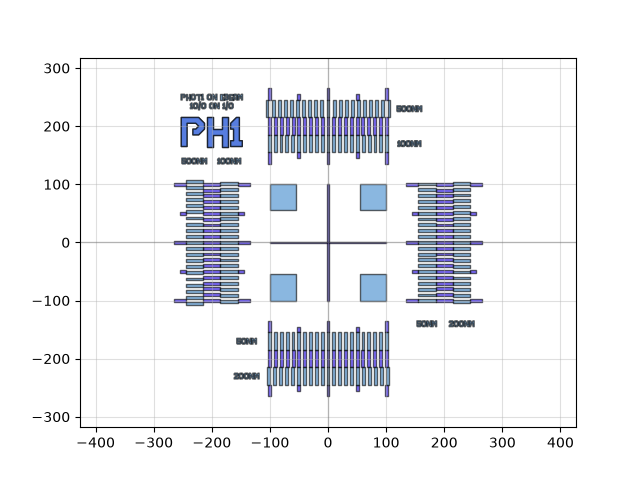
- qnngds.test_structures.alignment_mark(layer1: LayerSpec = (1, 0), layer2: LayerSpec = (10, 0)) Device[source]
Creates vernier caliper comb between two layers.
Helper method for alignment_mark.
- Parameters:
layer1 (LayerSpec) – center comb GDS layer specification
layer2 (LayerSpec) – top/bottom comb GDS layer specification
- Returns:
(Device) – alignment cross with vernier calipers
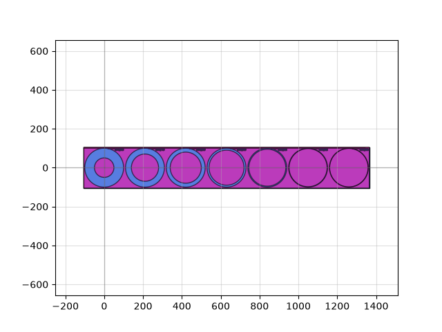
- qnngds.test_structures.circ_tlm(ext_radius: float = 100, int_radius: List[float] = [50, 70, 80, 90, 95, 98, 99], pad_layer: LayerSpec = (20, 0), mesa_layers: LayerSpecs = [(1, 0), (10, 0)], text_size: float = 10) Device[source]
Creates rectangular transfer-length-method test structures.
- Parameters:
ext_radius (float) – external radius of hole that defines outer pad
int_radius (List[float]) – list of internal radii. The gap is d = ext_radius - int_radius.
pad_layer (LayerSpec) – layer specification for probable pads.
mesa_layers (LayerSpecs) – layer(s) for bottom metal/semiconductor and/or vias
text_size (float) – size of text label
- Returns:
(Device) – TLM structure
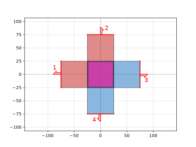
- qnngds.test_structures.cross_bridge_kelvin_resistor(size: float = 50, lead_length: float = 50, layer_top: LayerSpec = 'PHOTO1', layer_bot: LayerSpec = 'EBEAM_COARSE', layer_via: LayerSpec | None = 'PHOTO2') Device[source]
Generate a cross-bridge Kelvin resistor.
See this paper.
- Parameters:
size (float) – side length of square junction
lead_length (float) – length of leads to junction
layer_top (LayerSpec) – layer specification of top conductor
layer_bot (LayerSpec) – layer specification of bottom conductor
layer_via (LayerSpec | None) – if not None, create via on specified layer
- Returns:
(Device) – cross-bridge Kelvin resistor
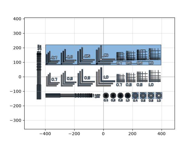
- qnngds.test_structures.dose_defocus(resolutions: tuple[float] = (0.7, 0.8, 0.9, 1.0), layer: LayerSpec = 'PHOTO1') Device[source]
Generate a test structure for doing dose/defocus tests
Contains a lithographic checkerboard, stars, crossed lines, and waffles.
- Parameters:
layer (LayerSpec) – layer to put pattern on
resolutions (tuple[float]) – resolutions to use for star, crossed lines and waffles. Resolution for litho checkerboard is determined automatically from maximum element.
- Returns:
(Device) – dose defocus test structure.
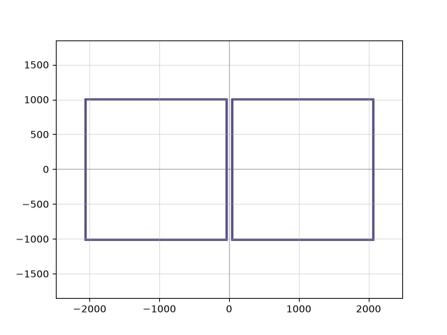
- qnngds.test_structures.etch_test(layer: LayerSpec = (1, 0), pad_size: tuple[float, float] = (2000, 2000), trench_width: float = 20) Device[source]
Construct side-by-side pads for performing electrical etch tests.
- Parameters:
layer (LayerSpec) – GDS layer specification
pad_size (tuple[float, float]) – width, height of each pad
trench_width (float) – width of trench around each pad
- Returns:
(Device) – etch test structure
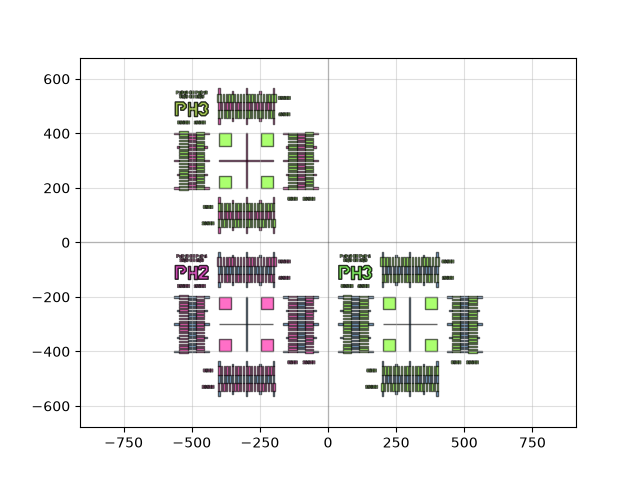
- qnngds.test_structures.multilayer_alignment(layers: LayerSpecs = ['PHOTO1', 'PHOTO2', 'PHOTO3']) Device[source]
Creates an alignment mark for each lithography layer.
- Parameters:
layers (LayerSpecs) – A list of GDS layer specifications
- Returns:
(Device) – alignment marks between each layer pair
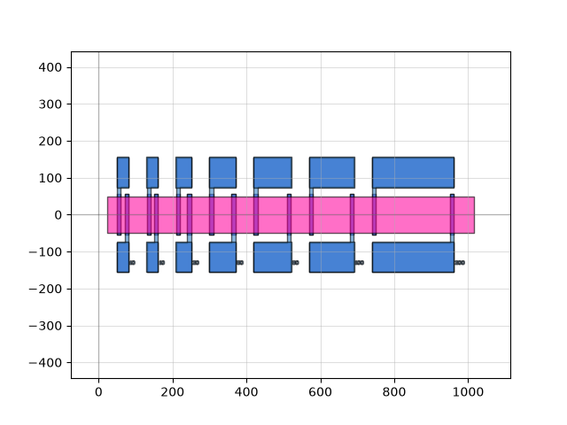
- qnngds.test_structures.rect_tlm(contact_l: float = 10, spacings: List[float] = [10, 10, 20, 50, 80, 100, 200], contact_w: float = 100, via_layer: LayerSpec | None = (1, 0), finger_layer: LayerSpec = (10, 0), pad_layer: LayerSpec | None = (10, 0), mesa_layer: LayerSpec = (20, 0), pad_size: Tuple[float, float] = (80, 80)) Device[source]
Creates rectangular transfer-length-method test structures.
- Parameters:
contact_l (float) – length of metal contact on semiconductor
spacings (List[float]) – list of spacings between contacts
contact_w (float) – width of contact/semiconductor
via_layer (LayerSpec | None) – layer specification for via between mesa and fingers. If None, don’t include via.
finger_layer (LayerSpec) – layer for fingers that periodically contact mesa
pad_layer (LayerSpec | None) – layer for probable pads. If None, don’t include.
mesa_layer (LayerSpec) – layer for semiconductor
pad_size (tuple(float,float)) – width, height of pad
- Returns:
(Device) – TLM structure
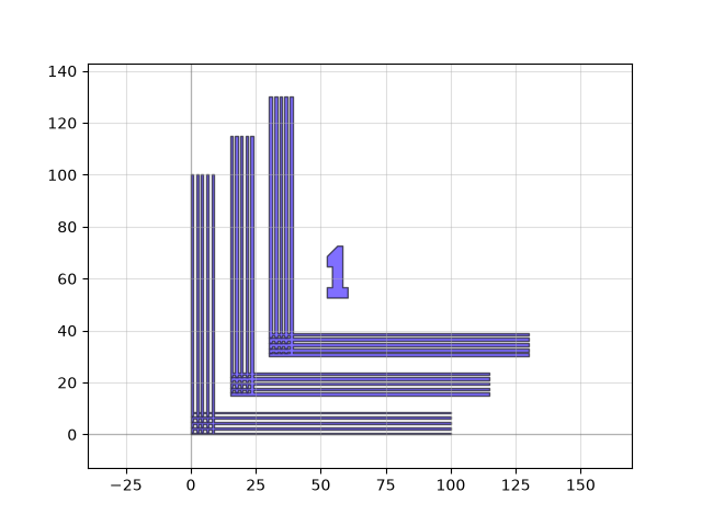
- qnngds.test_structures.resolution_L(res: float | int = 1, layer: LayerSpec = (1, 0)) Device[source]
Creates L-shaped test structures for determining process resolution.
Helper method for resolution_test.
- Parameters:
res (float or int) – Resolution (in µm) to be tested.
layer (LayerSpec) – GDS layer specification
- Returns:
(Device) – the resolution test structure
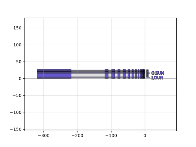
- qnngds.test_structures.resolution_checkerboard(resolutions: List[float] = [0.1, 0.2, 0.3, 0.4, 0.5, 0.6, 0.7, 0.8, 0.9, 1.0], layer: LayerSpec = (1, 0), label_interval: int = 5, label_size: float = 10) Device[source]
Creates crossed lith_steps pattern for lithographic resolution test.
- Parameters:
resolutions (List[float]) – List of resolutions (in µm) to be tested.
layer (LayerSpec) – GDS layer specification
label_interval (bool) – how often to label (set to 0 to disable all labels)
label_size (float) – size of text label
- Returns:
(Device) – the litho test structure
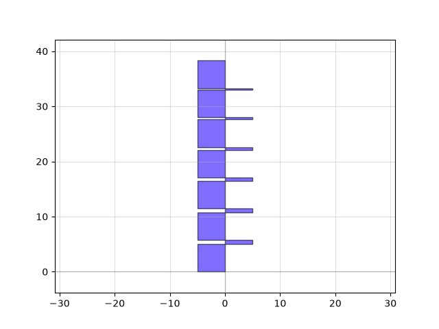
- qnngds.test_structures.resolution_steps(resolutions: List[float] = [0.3, 0.4, 0.5, 0.6, 0.7, 0.8], width: float = 5, spacing: float = 5, layer: LayerSpec = (1, 0)) Device[source]
Creates step pattern for lithographic resolution test.
Adapted from PHIDL.
- Parameters:
resolutions (List[float]) – List of resolutions (in µm) to be tested.
width (float) – width of stripes
spacing (float) – spacing between stripes
layer (LayerSpec) – GDS layer specification
- Returns:
(Device) – the test structure
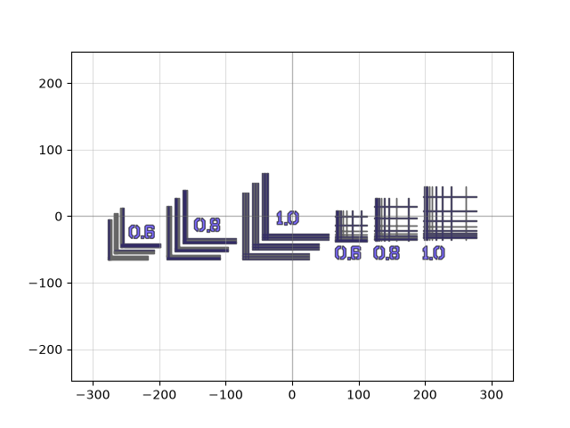
- qnngds.test_structures.resolution_test(resolutions: List[float] = [0.6, 0.8, 1.0], outline: float | None = None, layer: LayerSpec = (1, 0)) Device[source]
Creates L and waffle structures for determining process resolution.
- Parameters:
resolutions (List[float]) – List of resolutions (in µm) to be tested.
outline (Optional[float]) – If none, do not invert. If zero, invert the device, otherwise outline the device by this width.
layer (LayerSpec) – GDS layer specification
- Returns:
(Device) – the resolution test structures
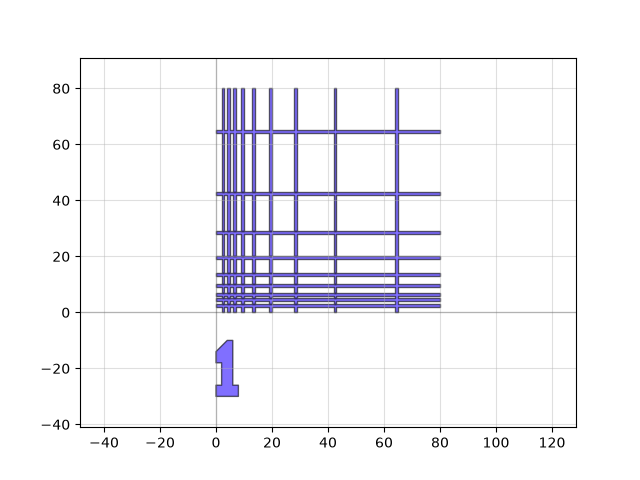
- qnngds.test_structures.resolution_waffle(res: float | int = 1, layer: LayerSpec = (1, 0)) Device[source]
Creates resolution_waffle test structures for determining process resolution.
Helper method for resolution_test.
- Parameters:
res (float or int) – Resolution (in µm) to be tested.
layer (LayerSpec) – GDS layer specification
- Returns:
(Device) – the resolution test structure
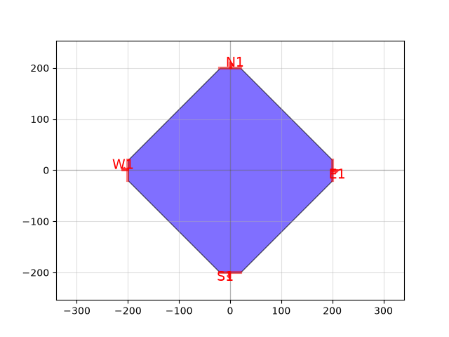
- qnngds.test_structures.vdp(diagonal: float = 400, contact_width: float = 40, layer: LayerSpec = (1, 0)) Device[source]
Creates a Van der Pauw (VDP) device with specified dimensions.
- Parameters:
diagonal (float) – Length of the VDP device, overall maximum dimension, in µm.
contact_width (float) – Width of the contact points (width of the ports), in µm.
layer (LayerSpec) – GDS layer specification
- Returns:
(Device) – Van der Pauw cell
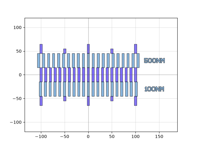
- qnngds.test_structures.vernier_comb(pitch1: int | float = 0.5, pitch2: int | float = 0.1, layer1: LayerSpec = (1, 0), layer2: LayerSpec = (10, 0), text_angle: int | float = 0) Device[source]
Creates vernier caliper comb.
Helper method for alignment_mark.
- Parameters:
pitch1 (int or float) – pitch of top comb
pitch2 (int or float) – pitch of bottom comb
layer1 (LayerSpec) – center comb GDS layer specification
layer2 (LayerSpec) – top/bottom comb GDS layer specification
text_angle (int or float) – angle to rotate text labels
- Returns:
(Device) – alignment vernier calipers
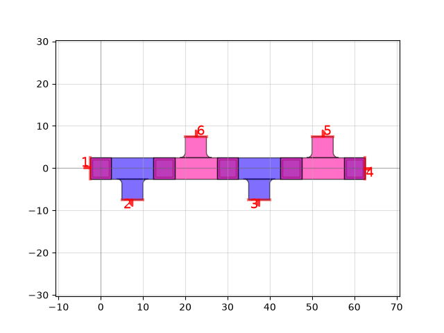
- qnngds.test_structures.via_chain(via_spec: DeviceSpec | Device = <function via>, num_vias: int = 5, spacing: float = 10, tap_period: int = 1) Device[source]
Makes a chain of vias, with optional taps along the length of the chain.
- Parameters:
via_spec (DeviceSpec | Device) – function, component name, or component for the via
num_vias (int) – number of vias to include in chain
spacing (float) – spacing between vias
tap_period (int) – number of vias between each tap. If zero, doesn’t place any taps.
- Returns:
(Device) – the via chain
typing
Custom types for Layers and Devices
LayerSpec: string, int, or tuple. int and tuple are pdk-agnostic, whereas string requires the a registered pdk to have a matching entry in its LayerSet.
DeviceSpec: string, callable, Device. Like with LayerSpec, string requires a registered pdk with matching Device name
CrossSectionSpec: string, callable, CrossSection. Like with LayerSpec, string requires a registered pdk with matching CrossSection.
utilities
Utilities for modifying/combining devices into more complex devices or constructing experiments.
- qnngds.utilities.extend_ports(device: Device, port_names: Sequence[int | str], extension: DeviceSpec, auto_width: bool = False, new_ports: bool = True, ext_swap_ports: bool = False, ext_mirror: tuple[tuple[float, float], tuple[float, float]] | None = None) Device[source]
Adds the DeviceSpec extension to the named ports of Device device
- Parameters:
device (Device) – device to add extensions to
port_names (Sequence[int | str]) – names of ports on device which should be extended
extension (DeviceSpec) – specification for extension
auto_width (bool) – if True, uses the kwarg start_width when instantiating the extension DeviceSpec to generate the tapers. Determines the start_width automatically from device.
new_ports (bool) – if True, create new ports, using port 2 from Device specified by extension. Also passes any non-extended ports through to the new device that is returned.
ext_swap_ports (bool) – if True, connects port 2 of the extension to the device instead of port 1.
ext_mirror (tuple[tuple[float, float], tuple[float,float]] | None) – if not None, mirror the extension along the vector ext_mirror.
- Returns:
(Device) – the original device with ports extended
- qnngds.utilities.create_layered_ports(device: Device, layer: LayerSpec)[source]
Regenerates new ports for device, assigning them all to a layer
- Parameters:
device (Device) – device to modify
layer (LayerSpec) – GDS layer specification
- qnngds.utilities.hyper_taper_fn(t: float, start_width: int | float, end_width: int | float) float[source]
Used for defining custom cross section widths/offsets
- Parameters:
t (float) – value on [0,1] mapping to position along length of taper
start_width (float) – starting width (t=0)
end_width (float) – ending width (t=1)
- Returns:
(float) – hyper taper function evaluated at t.
- qnngds.utilities.get_outline_layers(layer_set: LayerSet) dict[str, float][source]
Get dictionary maping each layer in a LayerSet to its desired outline amount
- Parameters:
layer_set (LayerSet) – LayerSet
- Returns:
(dict[str, float]) – mapping of GDS layer name to outline distance. Layers that aren’t outlined are omitted.
- qnngds.utilities.get_keepout_layers(layer_set: LayerSet) dict[str, str][source]
Get dictionary maping a layer to a second layer which it should serve as a keepout for
- Parameters:
layer_set (LayerSet) – LayerSet
- Returns:
(dict[str, str]) – mapping of GDS layer name to GDS layer name.
- qnngds.utilities.outline(device: Device, outline_layers: dict[str, float] | None = None, kl_tile_size: int | None = None, kl_precision: float = 0.0001) Device[source]
Outline polygons within device by layer.
- Parameters:
device (Device) – device to outline
outline_layers (dict[str, float]) – map of desired outline amount per layer. If a layer is omitted, it will not be outlined
kl_tile_size (int | None) – if not None, size of tile to divide geometry into for multithreaded execution
kl_precision (int | None) – precision for KLayout operation (equivalently, sets dbu for KLayout)
- Returns:
(Device) – the outlined device
- qnngds.utilities.invert(device: Device, ext_bbox_distance: dict[LayerSpec, float] = {}, kl_tile_size: int | None = None, kl_precision: float = 0.0001) Device[source]
Outline polygons within device by layer.
- Parameters:
device (Device) – device to invert
ext_bbox_distance (dict[LayerSpec, float]) – amount to expand bounding box for each layer. If a layer is omitted, it will not be inverted.
kl_tile_size (int | None) – if not None, size of tile to divide geometry into for multithreaded execution
kl_precision (int | None) – precision for KLayout operation (equivalently, sets dbu for KLayout)
- Returns:
(Device) – the inverted device
- qnngds.utilities.keepout(device: Device, outline_layers: dict[LayerSpec, float] | None = None, keepout_layers: dict[LayerSpec, LayerSpecs] | None = None, kl_tile_size: int | None = None, kl_precision: float = 0.0001) Device[source]
Apply keepout layers
- Parameters:
device (Device) – device to outline
outline_layers (dict[LayerSpec, float]) – map of desired outline amount per layer. If a layer is omitted, it will not be outlined
keepout_layers (dict[LayerSpec, LayerSpecs]) – map of desired layer(s) to keepout. If a keepout layer applies to a positive-tone layer (i.e. layer in outline_layers with non-zero outline), then the keepout regions will be unioned. If keepout layer applies to negative-tone (i.e. layer not in outline_layers), then the keepout region will be subtracted.
kl_tile_size (int | None) – if not None, size of tile to divide geometry into for multithreaded execution
kl_precision (int | None) – precision for KLayout operation (equivalently, sets dbu for KLayout)
- Returns:
(Device) – device with keepout applied
- qnngds.utilities.get_cross_section_with_layer(layer: LayerSpec = 'PHOTO1', default: CrossSectionSpec | None = None) CrossSectionSpec | None[source]
Find the cross section associated with the given layer, or default
- Parameters:
layer (LayerSpec) – layer specification to find cross section for
default (CrossSectionSpec | None) – default return value if cross section is not found
- Returns:
(CrossSectionSpec | None) – found cross section or default